The week started with introduction to the ABC of the electronics, voltage, current, resistor, capacitors, diods, PCB, three phase and single phase current etc.
I was prepared for the fact that electronics is not my forte and it will take a long for me to get things.
Setting the Machine
We at Vigyan Ashram Fab lab are using ROLAND MODELA machine to mill our PCBs, We are using the the offline version of Fab Module to make all the settings for milling the PCB
Fab modules is basically a program that runs on your computer which in turn runs various Fab machines such as the vinyl cutter, milling machine etc.
There is also an online version of Fab Modules available on the internet which uses the web browser.
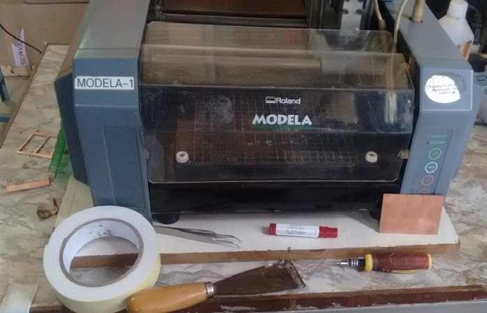
We at Vigyan Ashram are using FR 04 material to print the PCB, FR-4 (or FR4) is a grade designation assigned to glass-reinforced epoxy laminate sheets, tubes, rods and printed circuit boards (PCB). FR-4 is a composite material composed of woven fiberglass cloth with an epoxy resin binder that is flame resistant (self-extinguishing).
As a matter of fact we are using FR-1 material to print the PCB, FR-1 is a hard, flat material that consists of a thin layer of copper over a non-conductive phenolic resin.
Neil specifically mentioned that for FabLabs we use FR1 even though they are not as strong as the the FR4 but it mills beautifully and the endmill lasts longer
Second reason that we use FR1 over industrial standard FR4 is that the FR4 has a glass fiber reinforcement thus there is a constant fight between the material and the endmill, so you can make a few FR4 PCBs with the endmill before it is worn out
Third reason is that FR4 when milled produces glass fiber shreds which can be dangerous if inhaled, although they can sustain higher temperatures , at FabLab we dont go to that level of temperatures thus FR1 is fine for us.
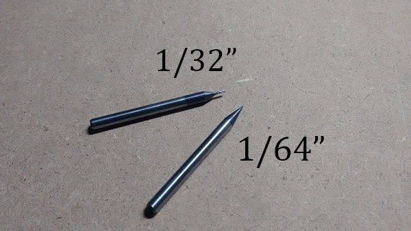
Besides this we are using two kinds of endmills, 1/64" for mmaking the traces to the boards and 1/32" to cut the boards.
/
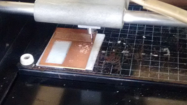
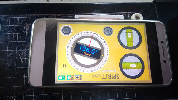
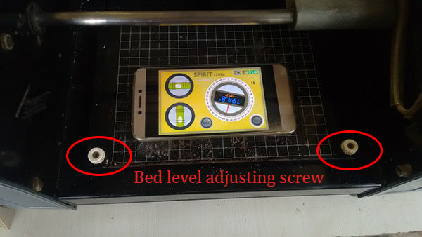
Before starting it is really important to have the bed levelled, Even a 1mm level difference is a huge difference when it comes to milling the PCBs, it will result in broken endmills or uneven PCB surface
I used an app on my phone to level the bed, this might not be a good idea (I believe there are better apparatus for this), It shows exactly the difference in the level of the bed
Now that the machine is levelled it is time to stick a double sided tape to the bed, this tape is going to receive the PCB from the top.
It is really important for the tape not to be too soft, if the tape is soft it will contract at the point where the endmill pierces the board, this will result in uneven PCB traces
As my evaluator suggested we can use/stick a sacrificial layer such as soft wood below the PCB, this will serve two purpose, one is that it will protect the machine if the mill depth goes beyond the PCB and the other is that it will give us a flat even surface so that the milling depth is the same everywhere unlike the sticky tapes which tend to deform with pressure
Also dont press down too hard on the tape, just gently play it with the tip of your fingers
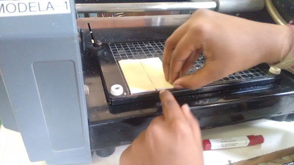
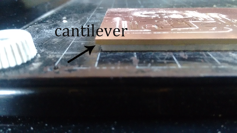
One piece of advice here could be that the sticking tape should cover the entire board, there should not be any cantilever left on the corners or the sides, This is because we usually slightly lower the endmill by gravity and if we lower it on the cantilever part which is usally lifted or sagged it will result in difference in level
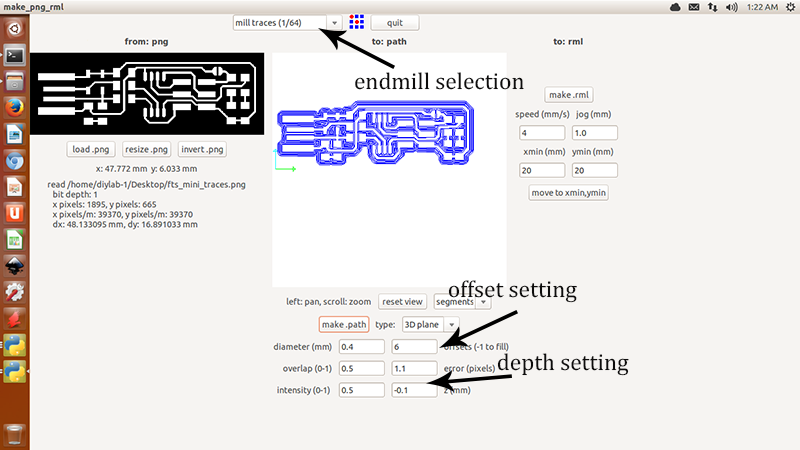
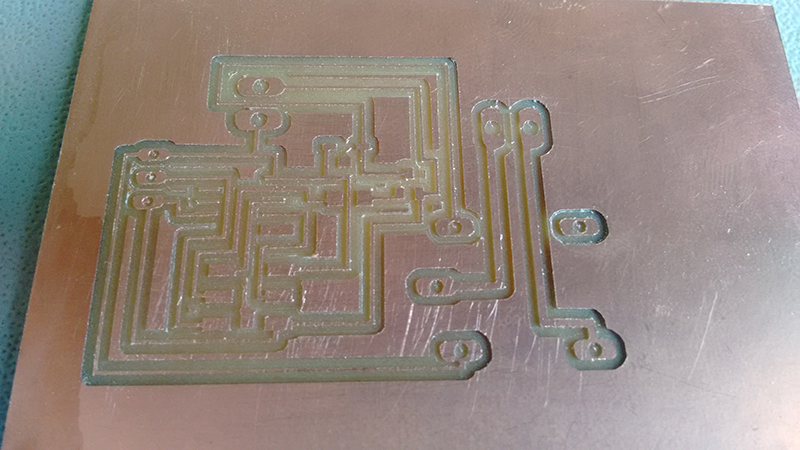
Now we move to the computer, I had already downloaded the .png image of the ISP I am making, I am following Brain's assignment page, this page gives us a detailed instructions.
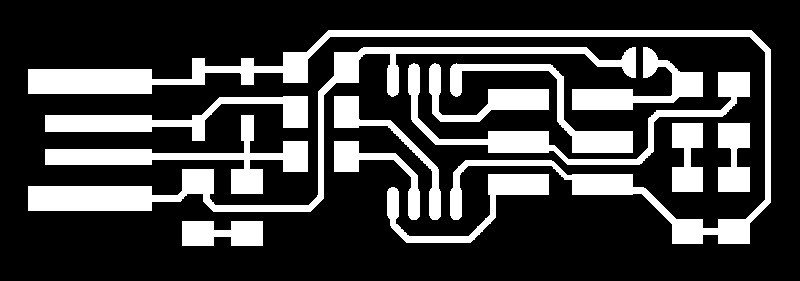

This is for the traces file
The machine has some basic settings which needs to be taken care of, once we import the file in the fabmodule. We have to select the endmill according to the process we want to do i.e if we want to make the traces we will select 1/64" endmill in the endmil selection tab, if we want to cut the pcb we will select 1/32" in the endmill selection.
Offset is the number of turns the endmill is going to take to make the track, this means more the offset cleaner the board. If the offset is really less eg 1/2 the board will have a lot of unwanted patches on it, this will cause you a lot while soldering the board, the solder will stick to such patches and make the board look dirty. This might also cause shorting of the traces
Depth settings deals with how deep the endmill goes while tracing, if the depth is too much the endmill will be subjected to a lot of forces, it will have to dig inside the PCB this might also result in the breaking of the endmill. The layers of the PCB after the copper layer are very hard made out of epoxy, it is realy not advisable to go deep in it. I would like to keep the depth -0.06 to -0.08 for my PCBs as this is the depth upto which the copper layer lies on the epoxy layer.
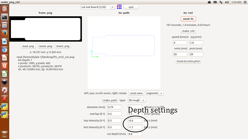
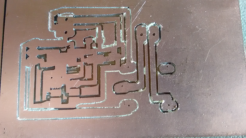
This is for the interior file
The same rules apply for the interior file, except for the fact that the depth is given in the range of the top and bottom z axis, care should be taken that too much depth is not given to the cut file even 1/32" endmill breaks if it has to plunge a lot at a time
Now that everything is done its time to move the endmill to the origin and lower itso that the tip is 10-15mm above the bed.
Now loosen the screw that holds the endmill in the chuck so that the endmill falls on the bed under gravity, if we have done this step correctly and if the horizontal levelof the PCB is correct without any cantilever there are a little chances that the PCB will turn out to be bad.
I have spoilt a lot of PCBs because of bad bed level or not setting the gravity correctly
 Difference is only because of bed bed level and not setting the endmill in the right position
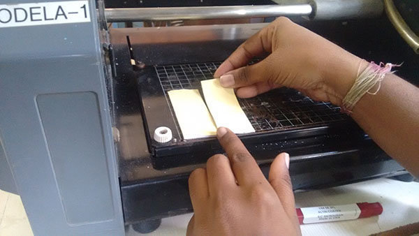
Try and use the PCB board wisely without any wastage.

 Courtesy Nishta Kaushik
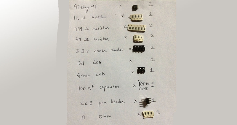
Its soldering time, I followed this sequence of soldering, this is fo the easy of working, first I soldered the Attiny 45, this one has 8 pads in total and it is necessary thta the IC should stick to all the 8 pads, next I soldered the diodes, resistors, capacitors and the LEDs, we really have to take care of the zener diodes, they get eaily spoilt if they are tempered with and at the last I soldered the ISP headers.
ISP header is a tough component to get it in the right place you will be tempted to solder it at the start but this will be a mistake, it is is a tall component it will come in the way while soldering the other components
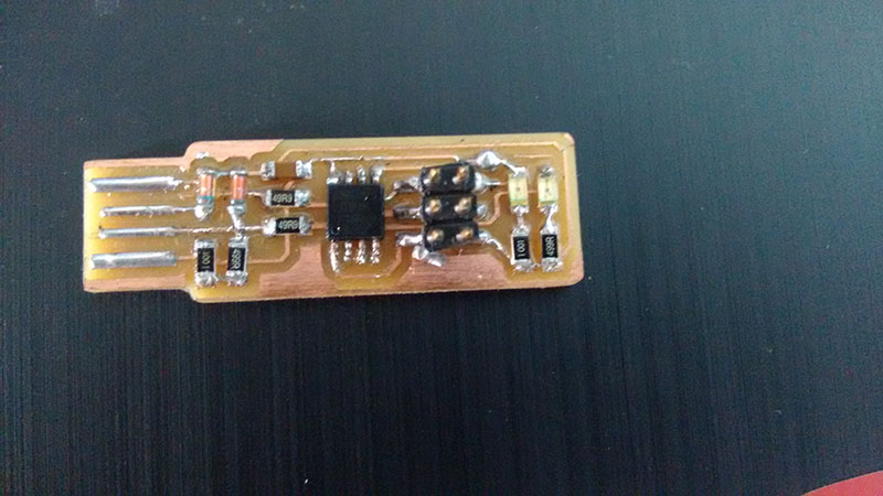
Once I got the board ready I checked it with a multimetre, I checked weather the LEDs are blinking, the resistance are showing the right values and there is continuity.
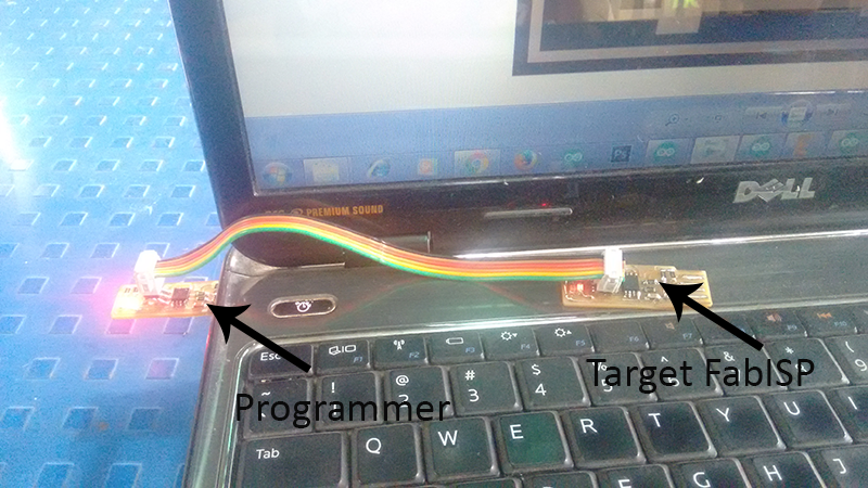
I programmed my board using an ISP of my instructer, I followed the instructions given by Brain in his assignment, I believe that is the best documentation I have found so far on the internet, so I am not going to repeat the same steps
It is not easy to get the board running in the first attempt, I made 4 FabISP boards and got the 4th one running after it was the fifth month of FabAcademy.
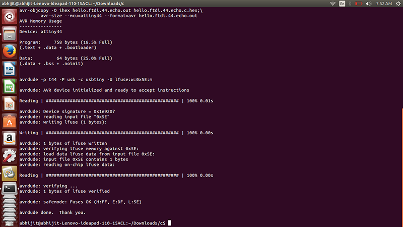
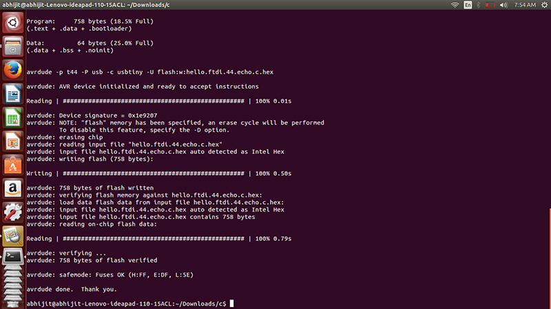
Only one advise I can give at this stage is to use sudo before all the functions such as "sudo make","sudo make flash", "sudo make fuses"
While programming the board it gives us an error to "double check the connections" sometime using sudo helps
 Happiest day of fabacademy
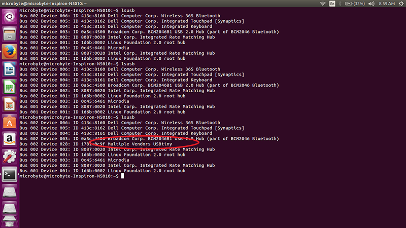
After everything was done I checked if my FabIsp is detected by the computer by typing lsusb in the terminal of ubuntu, it did show up
To set the reset disable so that the board cannot be programmed again I gave a command to resest disable make rstdisbl